


Written by Florida Wagers
Modified & Updated: 07 Dec 2024
Reviewed by Jessica Corbett
When it comes to the field of chemistry, there are countless fascinating phenomena and processes that capture the imagination of scientists and researchers. One such phenomenon is epitaxy. Epitaxy is a powerful technique used in the manufacturing of semiconductors and other electronic devices. Understanding epitaxy and its various applications can shed light on the advancements made in fields such as microelectronics and optoelectronics.
In this article, we will explore 19 surprising facts about epitaxy that will not only pique your interest but also deepen your understanding of this remarkable process. From its historical significance to its modern-day applications, we will delve into the intricacies of epitaxy and its impact on various industries. So, let’s embark on this scientific journey and uncover some intriguing facts about epitaxy!
Key Takeaways:
- Epitaxy is a crucial process in making electronic devices, like smartphones and solar panels, by growing thin films on a crystalline base. It helps improve their performance and efficiency.
- Epitaxy allows scientists to create unique materials with special properties, leading to advancements in electronics, optoelectronics, and even the emerging field of spintronics.
Epitaxy is a key process in semiconductor manufacturing.
Epitaxy is the method used to grow thin films of a material on a crystalline substrate, allowing for the precise control of film thickness and composition. It is crucial in the production of semiconductors used in electronic devices.
Epitaxy enables the creation of high-quality crystals.
By carefully controlling the growth conditions, epitaxy produces crystals with superior structural perfection compared to bulk materials. This results in improved electrical and optical properties, making epitaxial films highly desirable for various applications.
Epitaxy can be achieved through different methods.
There are various techniques used in epitaxy, including vapor phase epitaxy (VPE), molecular beam epitaxy (MBE), and chemical vapor deposition (CVD). Each method has its own advantages and is suited for specific applications.
Epitaxy allows for the creation of heterostructures.
Heterostructures are materials composed of layers with different properties. With epitaxy, it is possible to stack different semiconductor materials to create structures that exhibit unique electrical and optical characteristics.
Epitaxy plays a crucial role in the development of optoelectronic devices.
Optoelectronic devices, such as light-emitting diodes (LEDs), lasers, and photodetectors, rely on epitaxial layers to emit, detect, or control light. Epitaxy enables the precise tuning of materials for optimal device performance.
Epitaxy has revolutionized the field of microelectronics.
Thanks to epitaxy, the semiconductor industry has been able to continually push the limits of device performance and functionality. It has paved the way for advancements such as faster processors, higher-resolution displays, and smaller electronic components.
Epitaxy is used in the production of solar cells.
Photovoltaic cells used in solar panels often incorporate epitaxial layers to enhance light absorption and electron transport. This helps to improve overall solar cell efficiency.
Epitaxial growth can be influenced by strain.
The lattice mismatch between the substrate and the epitaxial layer can induce strain, affecting the properties of the grown film. Strained epitaxy is used to engineer unique electronic and optical effects in materials.
Epitaxy can be conducted at high temperatures.
Some epitaxial processes require high temperatures to ensure proper crystal growth. This can involve heating the substrate to several hundred degrees Celsius or even higher.
Epitaxy is widely used in the fabrication of integrated circuits.
The precise deposition of epitaxial layers is essential for the creation of transistors, interconnects, and other components in integrated circuits. Epitaxy enables the formation of well-controlled, highly uniform structures on a microscopic scale.
Epitaxial layers can be single crystal or polycrystalline.
Depending on the growth conditions, epitaxy can result in either a single crystal film with a continuous lattice structure or a polycrystalline film consisting of multiple small grains. The choice of film type depends on the specific application requirements.
Epitaxial films can be doped to alter their properties.
By introducing small amounts of impurities during the growth process, epitaxial films can be doped to modify their electrical conductivity or optical properties. This is crucial for tailoring materials for specific device functionalities.
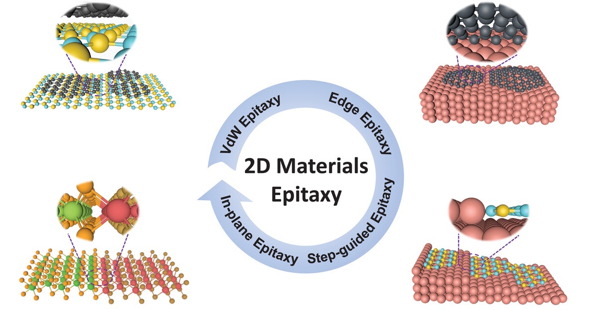
Epitaxy offers the potential for 2D material growth.
With the advent of 2D materials like graphene and transition metal dichalcogenides, epitaxy provides a promising avenue for their controlled growth. This opens up new possibilities in developing advanced electronic and optoelectronic devices.
Epitaxy is used in the production of semiconductor lasers.
The epitaxial growth of semiconductor materials is essential for manufacturing lasers used in telecommunications, medical applications, and optical data storage. Epitaxy ensures precise control over the active regions of the laser devices.
Epitaxial layers can be grown on various substrates.
While silicon is commonly used as a substrate in epitaxy, other materials like sapphire, gallium nitride, and indium phosphide can also serve as suitable substrates depending on the desired properties of the grown film.
Epitaxy plays a critical role in the development of quantum well structures.
Quantum well structures, consisting of ultra-thin epitaxial layers, exhibit quantum confinement effects that lead to unique electronic properties. These structures are utilized in various electronic and optoelectronic devices.
Epitaxial growth can be affected by surface preparation and cleanliness.
Prior to epitaxial growth, the substrate surface must be carefully prepared to ensure good quality film deposition. Any contaminants or irregularities can lead to defects in the epitaxial layers.
Epitaxy is advancing the field of spintronics.
Spintronics is an emerging field that utilizes the spin of electrons in addition to their charge for information processing and storage. Epitaxial growth of magnetic materials is crucial for building spintronic devices.
Epitaxial processes are constantly evolving and improving.
Researchers and engineers continue to refine epitaxial techniques and develop new materials, pushing the boundaries of what is possible in the realm of semiconductor technology. The future of epitaxy holds exciting possibilities for even more advanced electronic devices and applications.
Conclusion
Epitaxy is a fascinating field that has revolutionized the world of materials science and semiconductor technology. Through the controlled growth of thin films, epitaxy has allowed for the creation of advanced electronic devices with superior performance and functionality.
From its origins in crystallography to its applications in solar cells and LEDs, epitaxy has continually pushed the boundaries of what is possible in the world of electronics. The ability to precisely control the atomic arrangement of materials has paved the way for smaller, faster, and more energy-efficient devices.
As we continue to explore new materials and deposition techniques, epitaxy will undoubtedly play a pivotal role in shaping the future of technology. Its ability to engineer materials with tailored properties is opening up new avenues for innovation in fields such as quantum computing, nanotechnology, and wearable devices.
With its rich history and promising future, epitaxy remains a captivating area of study and research. Its impact on various industries continues to grow, and we can only speculate on the incredible advancements that lie ahead.
FAQs
1. What is epitaxy?
Epitaxy is the process of growing a crystalline film on a substrate in a controlled manner. It involves depositing atoms or molecules onto a substrate surface in such a way that they align with the existing lattice structure, resulting in a single crystal film.
2. What are the applications of epitaxy?
Epitaxy has a wide range of applications in various fields. It is extensively used in the semiconductor industry for fabricating high-performance electronic devices such as transistors, diodes, and integrated circuits. Epitaxy also plays a crucial role in the development of optoelectronic devices like lasers, LEDs, and solar cells.
3. How does epitaxy improve device performance?
Epitaxy enables the growth of high-quality crystals with controlled properties, such as defect density, composition, and strain. By precisely engineering these properties, epitaxy enhances device performance by improving carrier mobility, reducing energy losses, and increasing the efficiency of electronic and optoelectronic devices.
4. What are the different types of epitaxy?
There are several types of epitaxy, including molecular beam epitaxy (MBE), metal-organic vapor phase epitaxy (MOVPE), and chemical vapor deposition (CVD). Each method has its own advantages and is suitable for specific material systems and applications.
5. What is the future of epitaxy?
The future of epitaxy looks promising, with ongoing research focused on exploring new materials and deposition techniques. Epitaxial growth on two-dimensional materials, such as graphene, and the development of III-V semiconductor heterostructures for quantum computing are some of the exciting areas of investigation.
Epitaxy's fascinating world is just the beginning of a captivating journey through science and technology. Crystal growth holds its own set of intriguing secrets waiting to be discovered. Materials science surprises with its depth and breadth of influence on our daily lives. Nanotechnology astounds with its potential to revolutionize industries and shape our future. Dive deeper into these topics and uncover the hidden wonders that lie within.
Was this page helpful?
Our commitment to delivering trustworthy and engaging content is at the heart of what we do. Each fact on our site is contributed by real users like you, bringing a wealth of diverse insights and information. To ensure the highest standards of accuracy and reliability, our dedicated editors meticulously review each submission. This process guarantees that the facts we share are not only fascinating but also credible. Trust in our commitment to quality and authenticity as you explore and learn with us.