
Written by Linn Ables
Modified & Updated: 04 Mar 2024
Reviewed by Sherman Smith
Schottky barrier is a fascinating concept in the field of physics and materials science that has significant implications in various electronic devices and semiconductor technologies. It refers to the barrier formed at the junction between a metal electrode and a semiconductor material. This phenomenon was first discovered by Walter H. Schottky in the early 1930s, and since then, it has been extensively studied and utilized in numerous applications.
In this article, we will explore 11 extraordinary facts about the Schottky barrier that will enhance your understanding of its importance and relevance in modern technology. Whether you’re a chemistry enthusiast, a physics student, or simply curious about the inner workings of electronic devices, these intriguing facts will leave you amazed.
Key Takeaways:
- Schottky Barrier is a crucial component in electronics, offering low voltage drop, fast switching speeds, and high breakdown voltage. It is named after physicist Walter H. Schottky and finds use in various applications.
- With its unique properties, Schottky Barrier plays a vital role in modern integrated circuits and energy harvesting devices. It ensures efficient power conversion and consistent performance across a wide range of temperatures.
Schottky Barrier is named after Walter H. Schottky
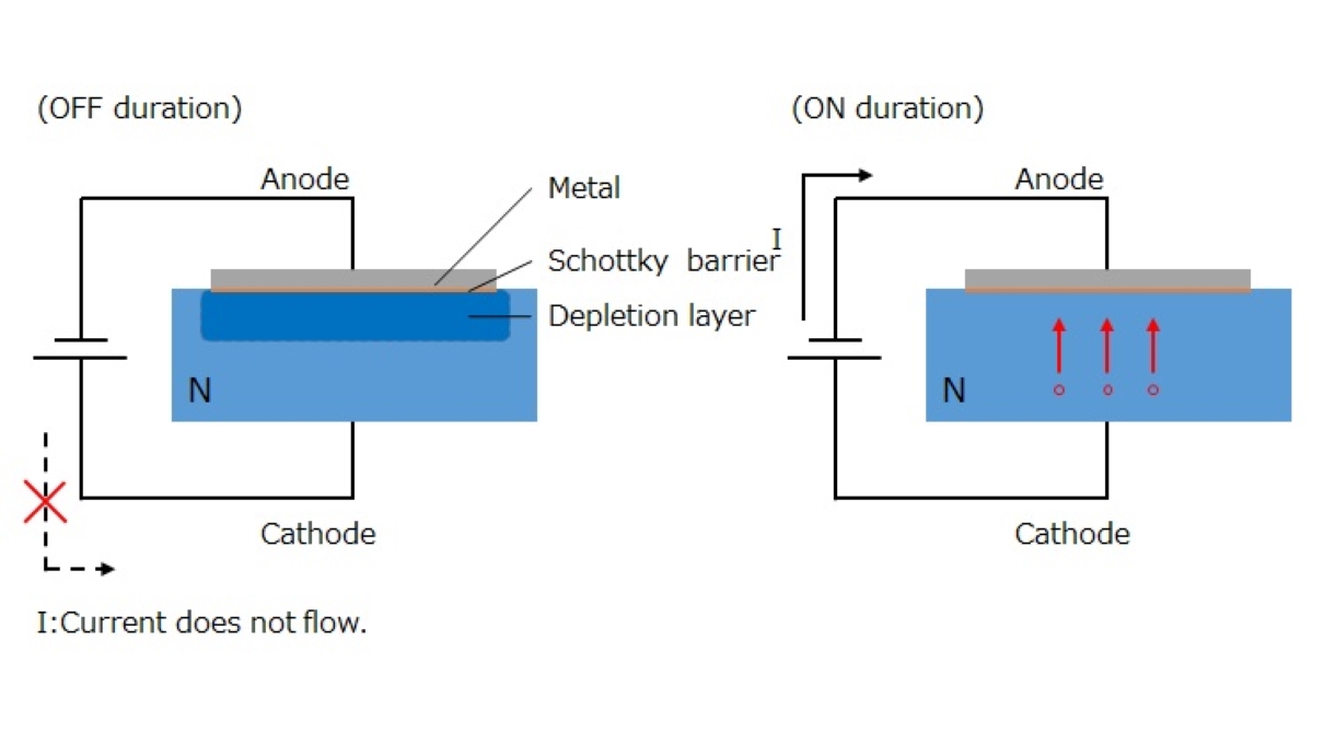
The Schottky Barrier gets its name from the German physicist Walter H. Schottky, who first described the phenomenon in the early 20th century. The Schottky Barrier refers to the potential energy barrier that forms at the interface between a metal and a semiconductor material.
It is commonly used in electronic applications
The Schottky Barrier has found wide-ranging applications in the field of electronics. It is commonly used as a rectifying contact in devices such as diodes, solar cells, and transistors. The unique properties of the Schottky Barrier make it ideal for high-frequency and high-speed applications.
It exhibits low forward voltage drop
One of the remarkable characteristics of the Schottky Barrier is its low forward voltage drop. This means that it can conduct current more efficiently compared to other types of contacts, leading to reduced power losses and improved overall efficiency in electronic devices.
Schottky Barrier diodes have fast switching speeds
Schottky Barrier diodes are known for their speedy switching capabilities. Due to the absence of minority carrier storage in the metal-semiconductor junction, Schottky diodes can quickly transition between conducting and non-conducting states, making them ideal for high-frequency applications.
It has high breakdown voltage
Schottky Barrier devices exhibit high breakdown voltage properties, which allow them to handle significant amounts of voltage without experiencing excessive electrical breakdown or failure. This makes them suitable for use in power electronics and high-voltage applications.
The Schottky Barrier has a low Reverse Recovery Time
Unlike conventional p-n junction diodes, Schottky Barrier diodes have a significantly shorter Reverse Recovery Time (TRR). This characteristic ensures minimal loss of energy during the transition from the conducting to the non-conducting state, making them advantageous in switching applications.
It is used in energy harvesting devices
Schottky Barrier diodes are widely employed in energy harvesting devices such as solar panels. Due to their low forward voltage drop and fast switching speeds, they efficiently convert solar energy into usable electrical power, contributing to the sustainable production of clean energy.
Schottky Barrier transistors offer high-frequency performance
Schottky Barrier transistors, also known as Schottky Field-Effect Transistors (FETs), are renowned for their exceptional high-frequency performance. These devices enable the amplification and switching of signals at extremely high frequencies, making them valuable in wireless communication systems.
It has superior temperature stability
The Schottky Barrier exhibits excellent temperature stability compared to other types of contacts. This characteristic allows electronic devices incorporating Schottky diodes or transistors to maintain consistent performance across a wide range of operating temperatures.
Schottky Barrier devices have low parasitic capacitance
Schottky Barrier devices possess low parasitic capacitance, thanks to the absence of minority carrier injection and storage. This property minimizes unwanted signal loss and distortion, contributing to improved signal integrity and overall device performance.
The Schottky Barrier is crucial in modern integrated circuits
The Schottky Barrier plays a vital role in the development of modern integrated circuits. Its unique characteristics, including low voltage drop, fast switching speeds, and high-frequency capabilities, make it an essential component for optimizing the performance and efficiency of various electronic systems.
In conclusion, the 11 Extraordinary Facts About Schottky Barrier highlight its importance in the field of electronics. Named after Walter H. Schottky, the Schottky Barrier exhibits low forward voltage drop, fast switching speeds, high breakdown voltage, and low parasitic capacitance. It finds extensive use in various applications, including energy harvesting devices, power electronics, and integrated circuits. It is a remarkable electronic component with unique properties that contribute to improved device performance and efficiency.
Conclusion
Schottky barriers are a fascinating phenomenon in the field of semiconductor physics. Their unique characteristics and widespread applications make them an important topic of study. From their role in rectifying electrical currents to their contribution to the development of high-frequency devices, Schottky barriers have revolutionized various industries.
Understanding the extraordinary facts about Schottky barriers allows us to appreciate their significance in technological advancements. Their ability to enable fast switching and reduce power dissipation has made them essential in modern electronics. As researchers continue to explore the intricacies of Schottky barriers, we can expect further breakthroughs and innovations in the field.
FAQs
1. What is a Schottky barrier?
A Schottky barrier refers to the potential energy barrier formed at the interface between a semiconductor and a metal. It inhibits the flow of current in one direction while allowing it to pass in the other direction.
2. How does a Schottky barrier differ from a p-n junction?
Unlike a p-n junction, which forms through the diffusion of dopants into a semiconductor, a Schottky barrier occurs when a metal and a semiconductor come into contact. The formation mechanism and electrical behavior of these two types of junctions are different.
3. Can a Schottky barrier be used as a rectifier?
Yes, Schottky barriers are commonly used as rectifiers due to their ability to quickly switch on and off, allowing them to rectify electrical currents with high efficiency.
4. What are some applications of Schottky barriers?
Schottky barriers find applications in various fields such as power electronics, telecommunications, and optoelectronics. They are used in diodes, transistors, solar cells, and microwave devices.
5. Can Schottky barriers be tuned or modified?
Yes, the electrical properties of Schottky barriers can be modified by adjusting the material choices, doping levels, and interface engineering techniques. This flexibility allows for customized designs to suit specific applications.
6. Are Schottky barriers only formed between certain materials?
No, Schottky barriers can be formed between a wide range of metal-semiconductor combinations. While some combinations exhibit better performance characteristics, the phenomenon can be observed in various material pairings.
Schottky Barriers are just one fascinating aspect of the world of electronics. Dive deeper into this captivating field by exploring mind-blowing semiconductor facts that will leave you amazed. Uncover astonishing truths about diodes, the unsung heroes of electronic circuits. Finally, expand your knowledge with a treasure trove of electronics facts that will spark your curiosity and ignite your passion for this ever-evolving domain.
Was this page helpful?
Our commitment to delivering trustworthy and engaging content is at the heart of what we do. Each fact on our site is contributed by real users like you, bringing a wealth of diverse insights and information. To ensure the highest standards of accuracy and reliability, our dedicated editors meticulously review each submission. This process guarantees that the facts we share are not only fascinating but also credible. Trust in our commitment to quality and authenticity as you explore and learn with us.