


Photolithography is a process used in microfabrication to pattern parts of a thin film or the bulk of a substrate. But what makes it so special? Photolithography enables the creation of intricate designs on tiny surfaces, essential for producing microchips, circuit boards, and various electronic components. This technique involves transferring a pattern from a photomask to a light-sensitive chemical photoresist on the substrate. The process is repeated multiple times to build complex layers. Photolithography has revolutionized the electronics industry, allowing for the miniaturization of devices and the advancement of technology. Curious about the details? Here are 25 fascinating facts about photolithography that will give you a deeper understanding of this critical technology.
What is Photolithography?
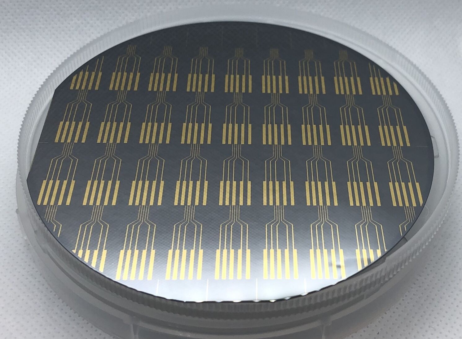
Photolithography is a process used in microfabrication to pattern parts of a thin film or the bulk of a substrate. This technique is crucial in the production of semiconductors and microchips. Here are some fascinating facts about photolithography.
- Photolithography is derived from Greek words meaning "light" and "stone writing."
- This technique was first developed in the 1950s for the semiconductor industry.
- Photolithography uses light to transfer geometric patterns onto a substrate.
- The process involves several steps, including cleaning, photoresist application, exposure, development, etching, and stripping.
- It is essential for creating intricate patterns on silicon wafers, which are used in electronic devices.
The Role of Light in Photolithography
Light plays a crucial role in photolithography. Different wavelengths of light are used to achieve various levels of precision and detail.
- Ultraviolet (UV) light is commonly used in photolithography due to its short wavelength.
- Deep Ultraviolet (DUV) light allows for even finer patterning, down to nanometer scales.
- Extreme Ultraviolet (EUV) lithography is the latest advancement, enabling even smaller feature sizes.
- The wavelength of light used directly impacts the resolution of the patterns created.
- Photomasks, which contain the desired pattern, are used to selectively expose parts of the photoresist to light.
Materials Used in Photolithography
Various materials are used in the photolithography process, each serving a specific purpose.
- Photoresists are light-sensitive materials applied to the substrate.
- Positive photoresists become soluble when exposed to light, while negative photoresists become insoluble.
- Silicon wafers are the most common substrates used in photolithography.
- Anti-reflective coatings are applied to prevent light from reflecting off the substrate and causing pattern distortions.
- Developers are chemicals used to remove the exposed or unexposed photoresist, depending on the type.
Applications of Photolithography
Photolithography has a wide range of applications beyond just semiconductor manufacturing.
- It is used in the production of printed circuit boards (PCBs).
- Photolithography is essential in the creation of microelectromechanical systems (MEMS).
- The technique is also used in the fabrication of optical devices, such as lenses and mirrors.
- Photolithography plays a role in the development of nanotechnology and nanodevices.
- It is used in the production of flat-panel displays, including LCDs and OLEDs.
Challenges and Innovations in Photolithography
Despite its importance, photolithography faces several challenges that drive continuous innovation.
- Achieving smaller feature sizes requires increasingly shorter wavelengths of light.
- The cost of photolithography equipment and materials is high, making it a significant investment.
- Maintaining precision and accuracy at the nanoscale is a constant challenge.
- Innovations such as immersion lithography, where the space between the lens and wafer is filled with liquid, help improve resolution.
- Researchers are exploring alternative techniques, such as electron beam lithography and nanoimprint lithography, to overcome current limitations.
The Final Snapshot
Photolithography, a cornerstone of modern technology, shapes our digital world. From its origins in the 19th century to its pivotal role in producing microchips, this process has revolutionized electronics. It’s fascinating how light and chemicals create intricate patterns on silicon wafers, enabling the production of smaller, faster devices.
Understanding photolithography helps appreciate the complexity behind everyday gadgets. Smartphones, computers, and even medical devices rely on this technology. As advancements continue, photolithography will push the boundaries of what's possible, driving innovation in various fields.
Whether you're a tech enthusiast or just curious, knowing these facts about photolithography offers a glimpse into the marvels of modern engineering. It’s a testament to human ingenuity and the relentless pursuit of progress. Keep exploring, stay curious, and marvel at the wonders of technology shaping our future.
Was this page helpful?
Our commitment to delivering trustworthy and engaging content is at the heart of what we do. Each fact on our site is contributed by real users like you, bringing a wealth of diverse insights and information. To ensure the highest standards of accuracy and reliability, our dedicated editors meticulously review each submission. This process guarantees that the facts we share are not only fascinating but also credible. Trust in our commitment to quality and authenticity as you explore and learn with us.